Centura
Exploring the Benefits of the Applied Materials AMAT Centura
Jan
Intro to Applied Materials AMAT Centura
Are you looking for a groundbreaking solution that can take your semiconductor manufacturing processes to new heights? Look no further than Applied Materials Centura.
AMAT Centura is a versatile platform that can handle a variety of critical processes effortlessly, making it a Swiss Army knife for the industry.
But what sets Centura apart from its competitors? How can it revolutionize your business and drive innovation in the industry?
In this discussion, we will explore the advanced technology, efficient processes, and global impact of Applied Materials Centura, giving you a glimpse into the transformative power it holds.
Prepare to unlock a world of possibilities as we delve into how Centura can enhance your device production and elevate your operations to the next level.
Advanced Technology
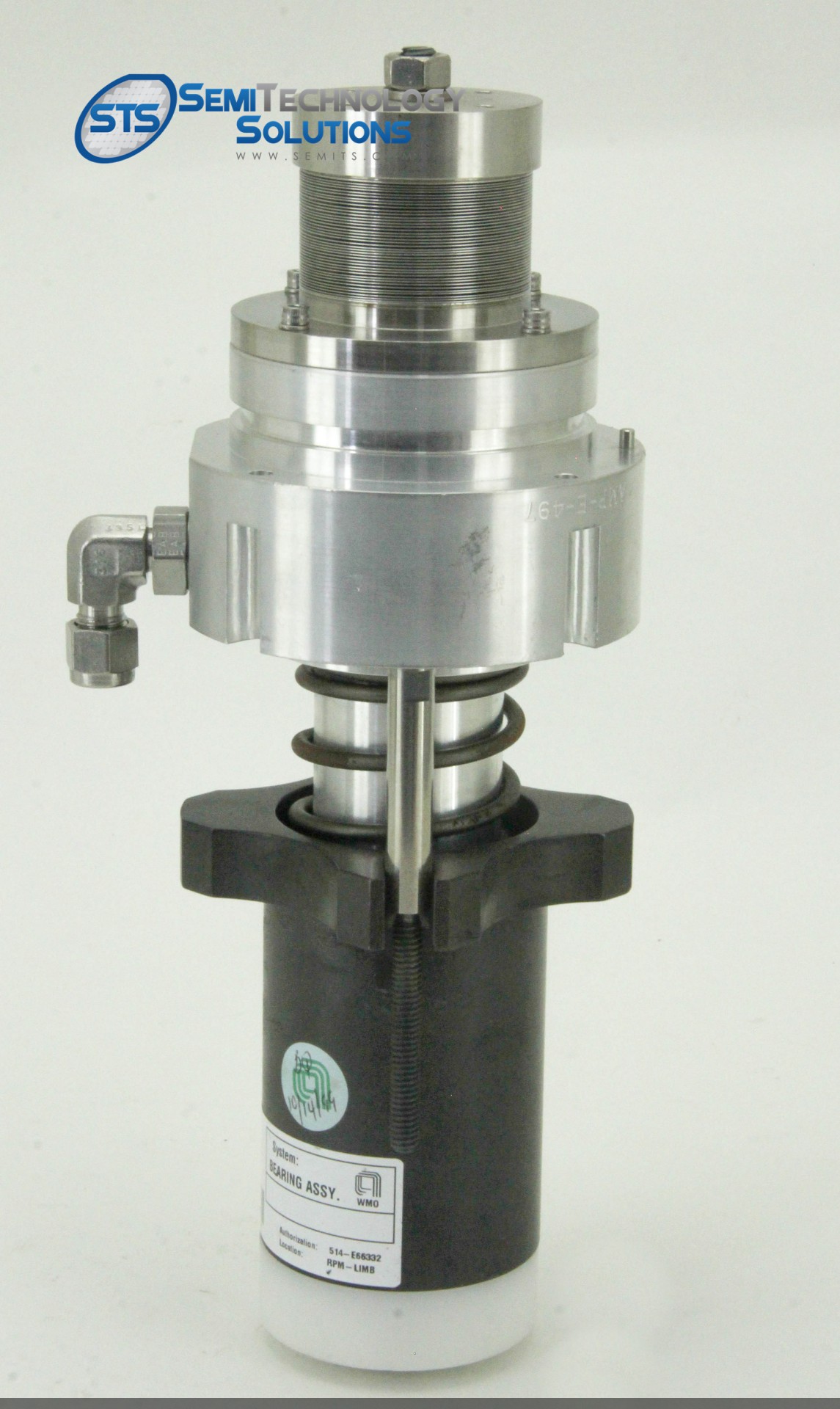
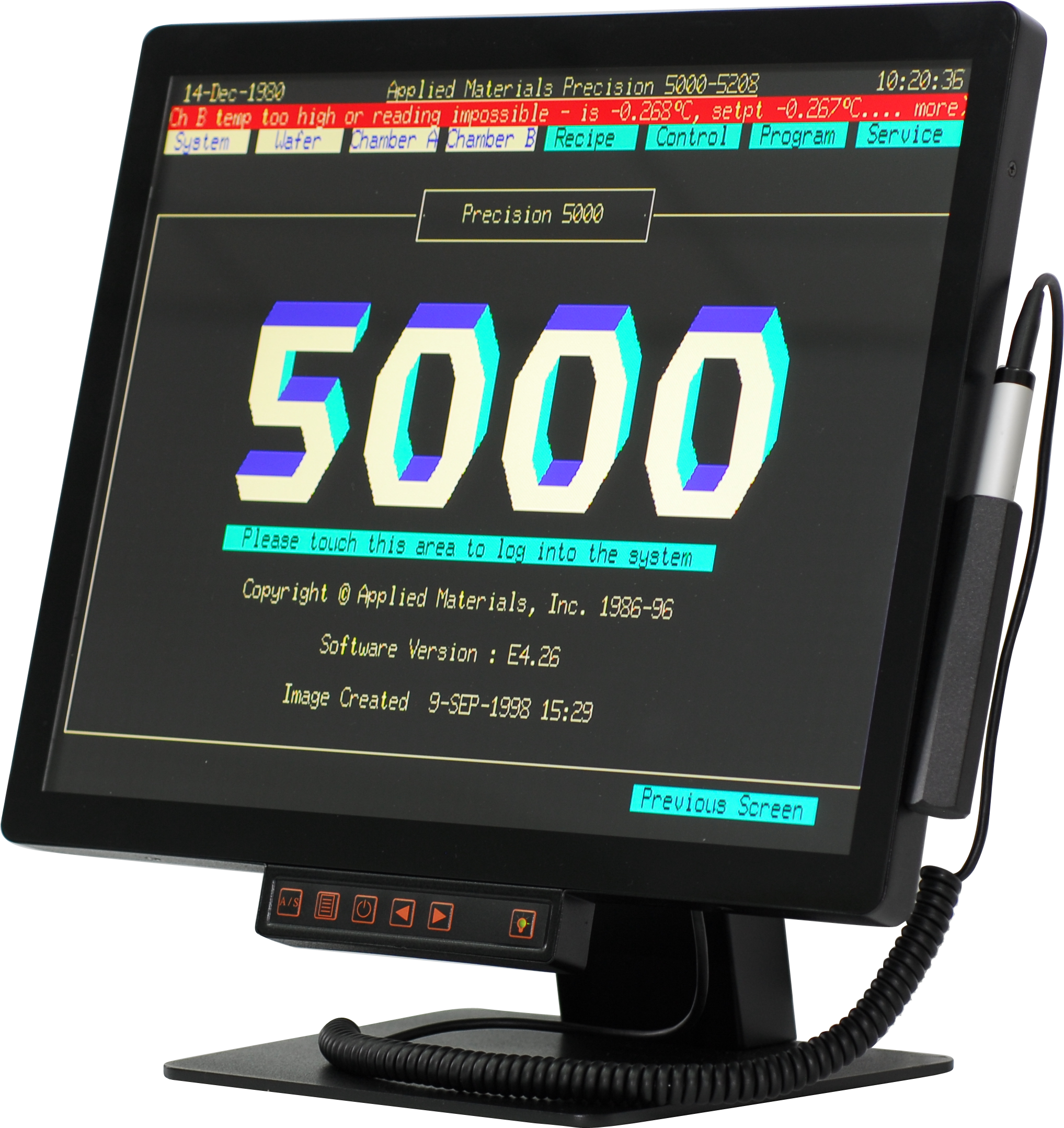
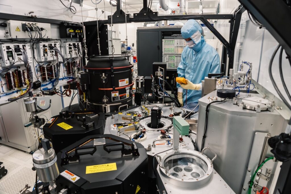
The AMAT Centura Etch System is a state-of-the-art tool for semiconductor production. It incorporates advanced technology to achieve precise control of critical dimensions in the manufacturing process.
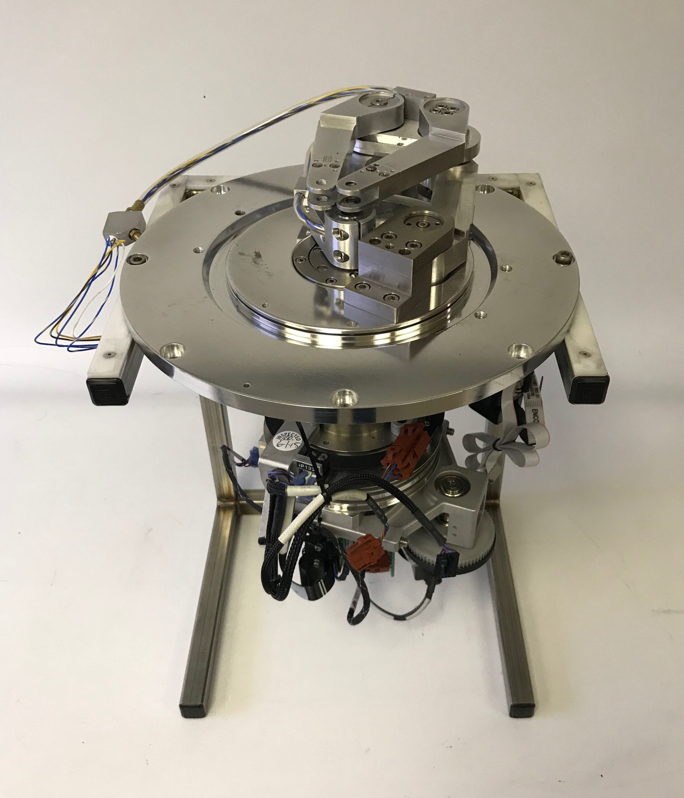
The Centura system features reactive ion etch (RIE) and metal etch capabilities, which are essential for achieving high aspect ratio etching and supporting materials like indium tin oxide, silicon carbide, and gallium nitride.
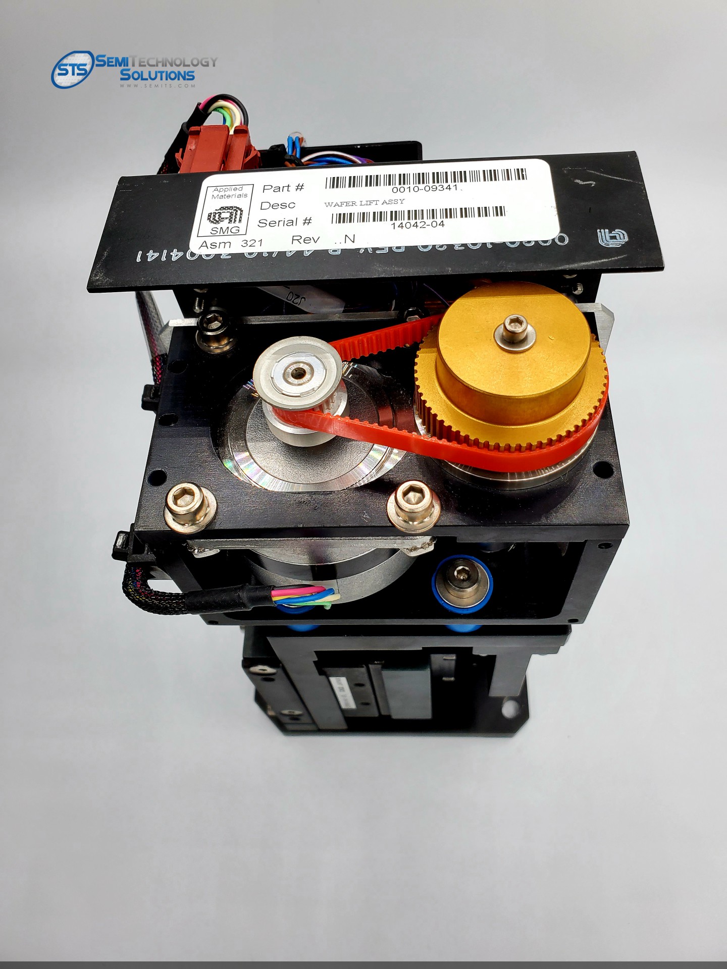
It’s equipped with process chambers designed to meet the specific needs of different wafer sizes, such as the Centura DPSDTM system for 150/200mm wafers and the Centura AP mainframe chamber technologies for 200/300mm wafers. These chambers offer flexibility and ensure accurate control of etch processes, enabling the production of high-quality semiconductor devices.
The Centura Etch System is a reliable and efficient tool that utilizes advanced technology to meet the demands of semiconductor manufacturing.
Efficient Processes
The Applied Materials Centura Etch System is a highly efficient solution for semiconductor manufacturing. It incorporates advanced technology and precise control of etch processes to improve productivity and enhance efficiency. This system is designed for 150mm and 200mm wafer sizes, allowing for integrated, sequential wafer processing in up to four process chambers.
One of the key features of the Centura Etch System is its ability to achieve high aspect ratio capability and high throughput. This is made possible by precisely controlling etch wall smoothness and trench profile. With this level of control, the system can handle various materials like indium tin oxide, silicon carbide, InGaAlP, GaAs, and gallium nitride.
In addition to the Centura Etch System, Applied Materials also offers the Centura Ultima HDP CVD. This part of the Centura system utilizes high-density plasma treatment to improve film quality. By extending the system’s lifespan and enhancing productivity and cost-efficiency, the Centura Ultima HDP CVD is a valuable addition to semiconductor manufacturing processes.
Furthermore, Applied Materials has collaborated with Intel Corp to develop the Centura Sculpta. This chip tool specifically targets the lithography process, lowering its cost while saving money, energy, and water. By providing a more cost-effective solution, the Centura Sculpta helps semiconductor manufacturers improve their bottom line.
Global Impact
The Applied Materials Centura Etch System has had a significant impact on the global semiconductor industry. This advanced system, offered by Applied Materials, Inc., is designed to address technology challenges and support the use of new materials in semiconductor manufacturing.
The AMAT Centura Etch System for 150/200mm wafers utilizes deep reactive ion etch (DRIE) technology, which allows for high aspect ratio capability and high throughput. This is crucial for creating intricate patterns and structures on semiconductor wafers.
For 200/300mm wafers, the AMAT Centura AP mainframe chamber technologies are used. These chambers support a wide range of materials and allow for sequential wafer processing in up to four process chambers. This enables efficient and streamlined production processes.
In addition to the Centura Etch System, Applied Materials also offers the Centura Ultima HDP CVD. This system provides superior gap-fill capability and film quality, ensuring the integrity and performance of semiconductor devices.
Furthermore, Applied Materials has introduced the AMAT Centura Sculpta chip tool, which aims to lower the cost of the lithography process. This has the potential to revolutionize chip manufacturing by making it more affordable and accessible.
Industry Transformation
The semiconductor industry is transforming to meet the demands of advanced technologies and the need for smaller, faster, and more efficient devices.
Applied Materials Centura Etch System is playing a crucial role in this transformation by providing a solution for achieving shallow junction MOSFETs, gates, transistor isolation trenches, and high aspect ratio contacts.
The Centura system, designed for 150mm and 200mm wafer sizes, supports integrated, sequential wafer processing in up to four process chambers.
Additionally, AMAT Centura Ultima HDP CVD system and Centura Sculpta chip tool are contributing to the industry’s transformation.
The Centura Ultima HDP CVD system offers high-density plasma CVD processes, while the Centura Sculpta chip tool is revolutionizing the lithography process.
These advancements are driving significant cost savings and increased efficiency in chip manufacturing.
Enhanced Device Production
Applied Materials’ Centura system is at the forefront of enhanced device production. This advanced system includes the Centura Etch System, which offers high-productivity etching for various materials, including silicon, metal, and dielectrics. It’s capable of handling high aspect ratio requirements, ensuring efficient production.
The Centura DPSDTM system utilizes deep reactive ion etch (DRIE) technology to achieve precise control of etch wall smoothness and trench profile. This enables high aspect ratio capabilities and high throughput.
The AMAT Centura AP mainframe chamber technologies provide precise control of etch processes for different materials, such as poly, metal, oxide, and DRIE. It supports both 200mm and 300mm wafer sizes, accommodating various manufacturing needs.
In addition, the Centura Sculpta, a new chip tool, utilizes plasma to shape a ribbon beam of light. This innovative approach has the potential to revolutionize the lithography process and drive advancements in chip manufacturing.
With its range of tools and technologies, the Applied Materials Centura system enhances device production by enabling efficient and precise manufacturing processes.
Wrapping Up
The Applied Materials AMAT Centura is a versatile and reliable system that caters to the needs of the semiconductor industry. With its advanced technology and efficient processes, Centura has the potential to revolutionize semiconductor manufacturing.
Professionals in the field can rely on Centura to enhance device production and allow for customization. Upgrade your operations and experience the benefits of the AMAT Centura platform firsthand.